연구개발
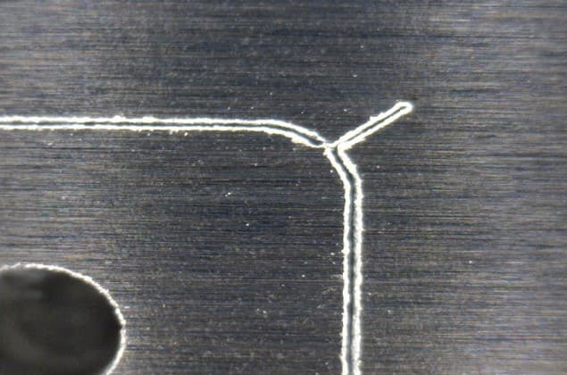
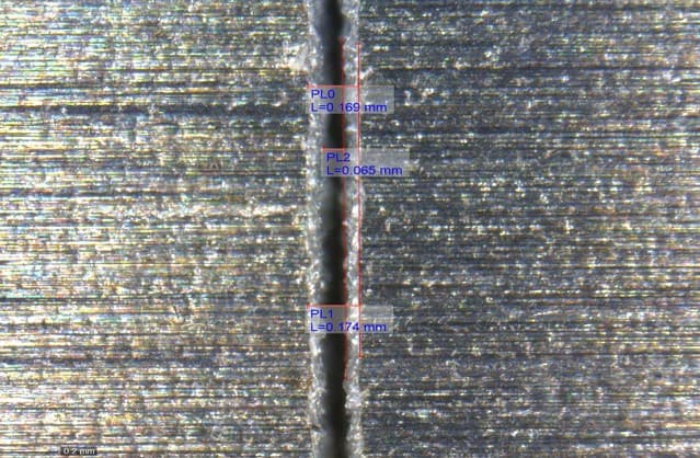
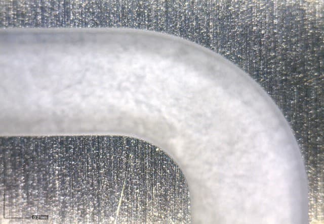
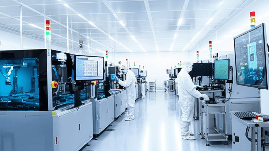
High Speed Laser Direct Imager
.avif&w=3840&q=75&dpl=dpl_n7KZ9G32dhvv1Btgk9bmRuTXjq85)
.avif&w=3840&q=75&dpl=dpl_n7KZ9G32dhvv1Btgk9bmRuTXjq85)
Competitiveness
In manual work with conventional UV scattered light, automated work is possible using a 405 nm laser light source
Can be minimised and microcircuited
Productivity and quality improvement
Fast productivity of 12 sec/side without the use of a separate master film
Blocking the foreign body funnel to improve the quality level
Vacuum Substrate Lamination using Equipment
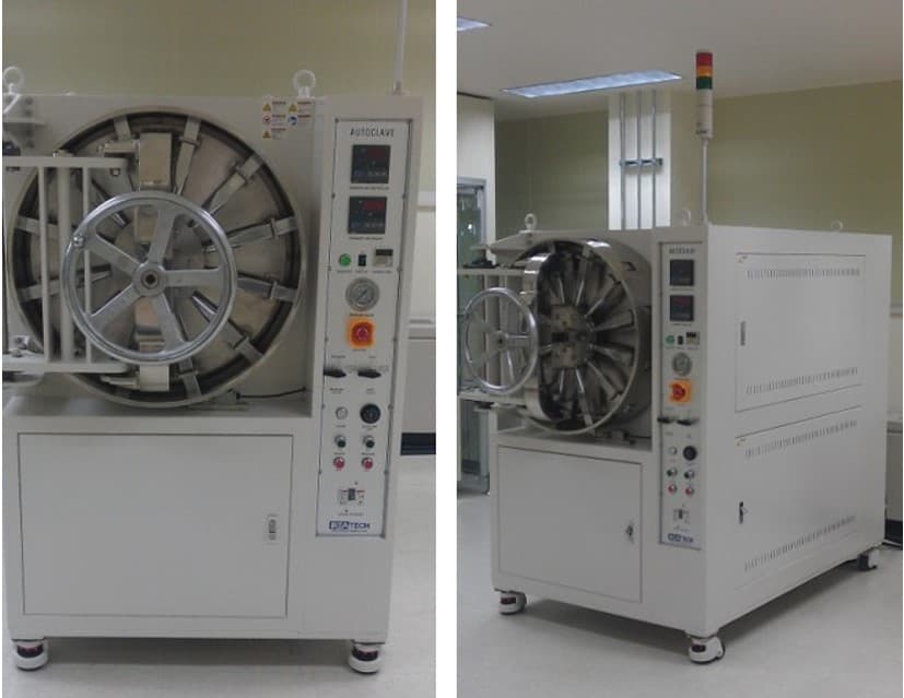
Competitiveness
Reduces product stress compared to traditional hot presses and quick presses
Solving resin problems with emissions and bubbles
Quality Improvement
Hot press, Reduces crack problems that are problematic during work
Pressurization using pressure and heat reduces bubble problems
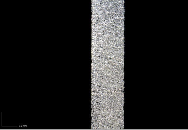
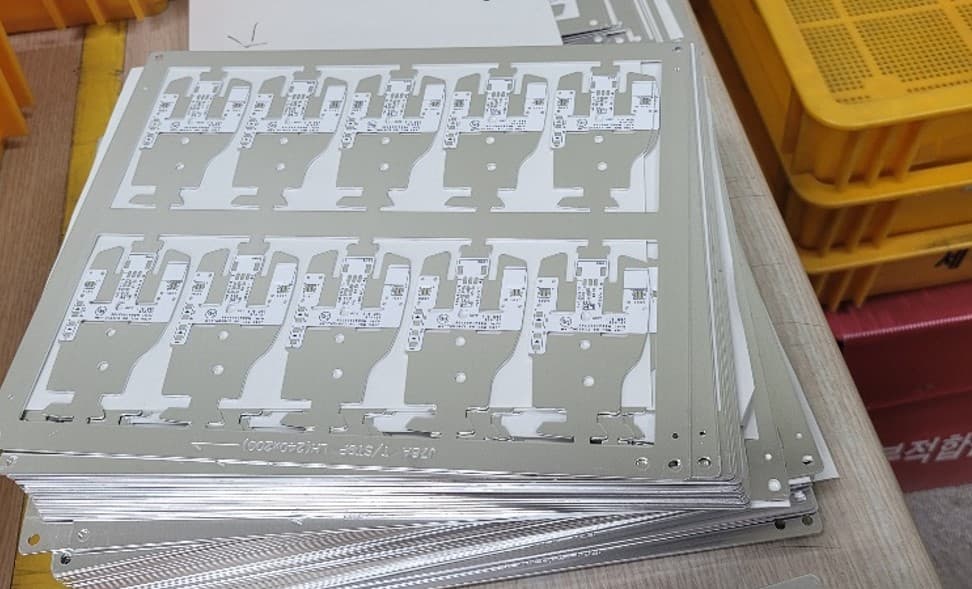
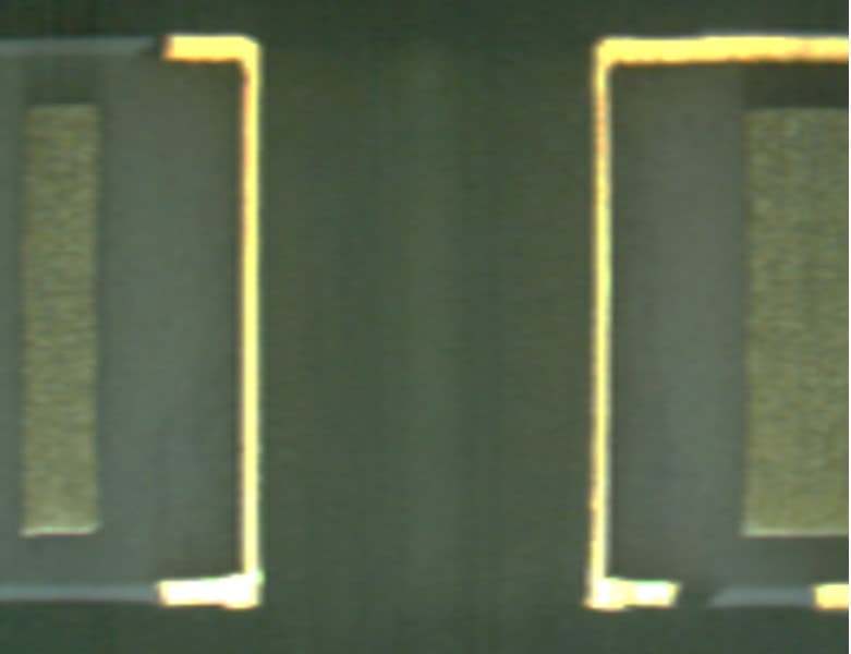
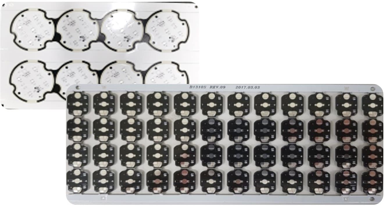
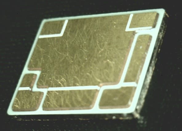
Insulator Filling Type Double-sided METAL PCB
Competitiveness
When the metal PCB is composed of two sides, the existing ink filling method has a long cost and process procedure
This is changed to the RCC filling method to simplify the process and strengthen reliability
Quality Improvement
Compared to Hole Plugging, RCC is used, which also increases fillability and resin curing
Copper plating and bondability improvement
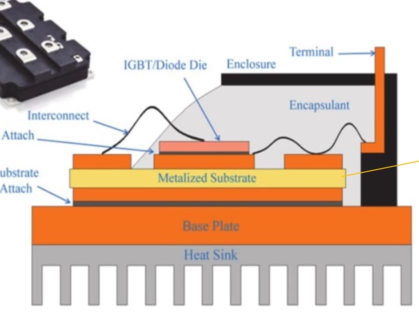
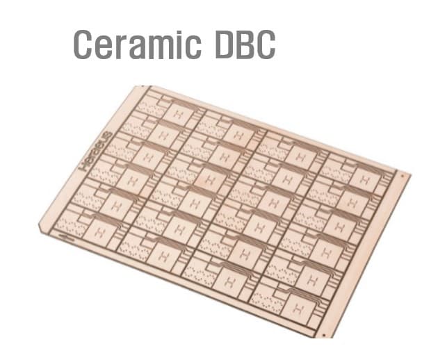
Replace Ceramic DBC : 9 Oz High heat dissipation IMS
Competitiveness
Securing a more simplified process of the existing ceramic DBC manufacturing process
Due to the characteristics of ceramics, it can compensate for the disadvantages of cracking and large-scale processing, opening up the existing DBC market
Development Challenges
Development of 5.0 W/mK ceramic resin insulation layer, which is an improvement over the existing 3.0 W/mK, is underway
6~9 Oz Heavy Copper, Development of circuit-forming machinability is underway
Laser Bridge Kit of Metal PCB